“To construct Gated SR-Latch using NAND Gate & To Verify its Different States”
“To construct Gated SR-Latch using NAND Gate & To
Verify its Different States”
1. Objective:
The main objective is to design and verify the different states of
i.
Gated SR
Latch using NAND Gate
2. Components:
i.
Bread Board
ii.
Connecting
Wires
iii.
2 LED’s
iv.
Battery
v.
IC for
NAND Gate
3. Introduction:
3.1.Bread Board:
A
bread board is an electronic board into which the electrical components like
diodes and resistors are placed. The sockets of bread board are sturdy and
rugged. Diodes or other electrical components should be placed without making
any damage to the board.
3.2.Integrated Circuits:
A circuit of transistors, resistors, and capacitors constructed on a single semiconductor wafer or chip, in which the components areinterconnected to perform a given function. IC’s consume very little current, generate comparatively
little heat, and are far more shock-proof and reliable than the older
discrete-component circuits.
An integrated circuit consists of a number of circuit components (e.g. transistors, diodes, resistors
etc.) and them inter connections in a single small package to perform a
complete electronic function. These components are formed and connected within
a small chip of semiconductor material. IC’s can be used as advanced logic
gates.
3.3.Light Emitting Diodes:
A light-emitting diode (LED) is a semiconductor device that emits visible
light when an electric current passes through it. LED’s
convert electrical energy to light energy. In electronics, polarity indicates whether a circuit component is symmetric or not.
Being diodes, will only allow current to flow in one direction. And when
there’s no current-flow, there’s no light. The positive side of the LED is
called the “anode” and is marked by having a longer
“lead,” or leg. The other, negative side of the LED is called the “cathode.”
3.4.SR-Latch:
A latch
is a fundamental component of data storage. A single latch can hold 1-bit of data,
increase that number by many orders of
magnitude and can create kilo, mega, giga, even terabytes of memory. Of course,
like most digital circuits, latches are made out of digital logic gates.
There are two controllable inputs: reset (R) and set (S), which produce the two
outputs: Q and Q(“Q-not”). That’s where the SR latch
get’s its name it’s a set/reset latch.
The SR latch comes with a
rule, which cannot ever be broken: Q must always be the
opposite of Q. These outputs are called complements. Here we made SR-Latch using following way:
3.4.1. SR-Latch
using NAND Gate:
To create an S-R latch, we can wire two NAND gates in
such a way that the output of one feeds back to the input of another, and vice
versa,
The Q and Q not outputs are supposed to be in opposite
states. Here making both the S and R inputs equal to 0 results in both Q and Q
not being 1. For this reason, having both S and R equal to 0 is called an invalid or illegal state for the S-R Latch using NAND
Gate. Otherwise, making S=0 and R=1 “sets” the Latch so that Q=1 and Q not =0.
Conversely, making R=1 and S=0 “sets” the Latch in the opposite state. When S
and R are both equal to 1, the Latch’s outputs in their prior states. This is
the No Change State. By definition, a condition of Q=1 and Q not=0 is set.
A condition of Q=0 and not-Q=1 is reset. These terms are universal in
describing the output states of any Latch circuit.
3.4.2. Gated SR Latch:
It is sometimes useful in logic circuits to have a
multivibrator which changes state only when certain conditions are met,
regardless of its S and R input states. The conditional input is called the enable,
and is symbolized by the letter E.
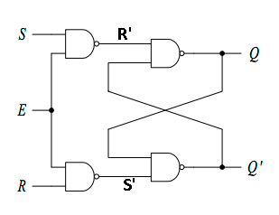
Gated SR- Latch can also be formed using NAND gates only in a
cross-coupled fashion. To accomplish this we need
to have an extra input pin called clock for enabling or disabling the latch.
When disabled, the previous states remain unchanged. Circuit that uses this
type of mechanism are called gated latches. In this case the circuit is called
Gated SR Latch. This latch is active low, that is when clock signal goes low
the Gated SR Latch behaves as a normal SR Latch. And when the clock signal goes high, whatever the logic at
inputs maybe, the output will remain the same unless and until the clock signal
goes low again.
4. Circuit Diagram:
5. Experimentation:
1. First of all, suitable IC for NAND gate is
chosen, i.e. IC 7400.
2. Inserted IC on the bread board.
3. As there are 14 pins on IC, 7th
pin is grounded and a positive potential is applied to the 14th pin
via a battery of potential less than 5V.
4. First Input S of first NAND is given the
input with battery and its second input is connected with the first input of
second NAND gate. Which is then connected to the negative terminal of the
battery so that Enable is on 0.
5. Second Input R of second NAND is connected
with the battery.
6. Output of first NAND gate is given to the
first input R’ of third NAND gate while output of second NAND is given to the
second input S’ of fourth NAND gate.
7. Second input of third NAND gate is connected
with the output Q’ of fourth NAND & the first input of fourth NAND Is
connected to the output of third NAND.
8. First LED is inserted on bread board with its
positive terminal connected to the output
of third NAND gate and negative signal is
given to the other terminal. Similarly Second LED is inserted on bread board
with its positive terminal connected to the output of fourth NAND gate and negative
signal is given to the other terminal.
9. Then one by one checked all the five possible
combination of S and R so as to verify the different states of Gated SR-Latch. Table
is verified and drawn.
6. Observations & Calculations:
The different states for SR-Latch using NAND is given below:
S
|
R
|
S'
|
R'
|
Q
|
Q'
|
State
|
0
|
1
|
0
|
1
|
0
|
1
|
Reset
|
0
|
0
|
1
|
1
|
0
|
1
|
No
Change
|
1
|
0
|
1
|
0
|
1
|
0
|
Set
|
0
|
0
|
1
|
1
|
1
|
0
|
No
Change
|
1
|
1
|
0
|
0
|
1
|
1
|
Invalid
|
7. Results & Discussion:
We have designed Gated SR-Latch using NAND Gates and the different
states are verified. We can deduce some main points from this. In the case of
NAND gate SR-Latch invalid state occur when both S & R are 1. In NAND gate
configuration 0,0 correspond to No Change State.
8. Conclusion:
Through this experiment we have designed Gated SR-Latch using NAND Gate
and its states are verified.
9. References:
I.
http://logic.ly/lessons/nor-gate/
VI.
http://elprojects.blogspot.com/2011/01/gated-sr-latch-using-nor-gates.html


Comments
Post a Comment